What a Counterfeit Lightning to Headphone Adapter Looks Like

Recently, I’d inadvertently bought a lightning to 3.5mm adapter that was a counterfeit. It wasn’t that obvious, but there are some tells externally. This was a good chance to compare with a genuine part and to see what’s going on inside.

Packaging

It’s not terribly obvious at first glance. The print quality seems equivalent, the card is right, the seals are in the right places. Looking closer, the easiest way is the subtle difference in the typeface and kerning. The ‘t’ is distinctly different, the kerning isn’t applied optically.

Physical

The genuine part has a very easy to identify raised molding around the lighting connector. Other than that, the precision of the molding on the fake part is considerably worse, with mold flash appearing around the connector.

X-Ray

  • The fake part uses 2 x QFN packages with only 4, possibly 5 external passives.
  • The genuine part uses a larger BGA on one side with a much smaller BGA on the other. There appears to be at least two 4-bump WCSP packages along with tens of passives.
  • There appears to be solder spatter on some of the wires on the fake part. This is generally found in a less well-controlled manufacturing process.
  • The wires are both more substantial and more carefully routed on the genuine part.
  • There is some mechanical reinforcement on the genuine part, a metal shroud underneath the molding. This could be to prevent stress around the PCB, particularly the BGA joints.
  • There are 7 wires on the genuine part and only 4 on the fake part from the lightning connector.

Performance

  • The dead giveaway, even without paying close attention to the packaging and build quality was the performance.
  • Listening at quieter volume levels clicks and pops were immediately obvious.
  • The 3.5mm jack socket created a scratchy noise on any physical movement.
  • After the first week, iOS starting throwing a “this accessory is not certified and may not work reliably with this iPhone”.

Other thoughts

I’d previously seen bad fakes online – usually, there are very obvious physical tells that the product isn’t genuine such as size, OEM-style packaging or markings. In this case, almost everything superficially appeared right until you look closer. I’d purchased from a seller on eBay (I know, I know…) with lots of positive feedback and assurances in the listing that it was genuine for £6. The price was the most obvious warning sign – a genuine part is £10. For more and more products these days I’d stick to buying from big-box retailers where there is more stringent sourcing, or straight from the manufacturer.

See also

Inside Apple’s New Audio Adapter
Apple Lightning to Headphone Jack Adapter Teardown
Adapter surgery

Generating Flat Flexible Soldered Cable Designs

The connection system (FFSC / Flat Flexible Soldered Cable?) described in my last post should allow for a high reliability, cost effective connection in medium to low density applications. To produce a similar design manually can be extremely time consuming due to the iterative nature of the problem.  If you need the design to be completely symmetrical then this process becomes harder. If you need to change something part way through, then really a piece of software to do it becomes essential.

The following Python script takes a set of parameters and generates an Eagle script to produce a FFSC design, including the top reinforcement layer. A basic example below:

ffsc-flat-flexible-soldered-connector-example-1

Almost all elements of the design can be adjusted to meet different applications, this includes all pad, track, spacing and reinforcement dimensions. Adjusting the length, taper and material thickness of the reinforcement layer allows you to get the mechanical gradient required for your application.

ffsc-flat-flexible-soldered-connector-example-2

For more involved applications, the script supports any number of segments to allow joining together of PCBs in non-parallel applications.

ffsc-flat-flexible-soldered-connector-example-3

The script is available to download from Github here.

Manufacturing

Whilst many design features of this connector type are new, the manufacturing processes required to make this connector are fairly standard. Most flex-capable PCB manufacturers should be able to produce this with a little thinking.

In volume, each layer is usually die cut out to the required shape before they are bonded together. In lower volumes or for prototyping purposes it may be possible to have each of these layers laser cut.

Flexible PCB connections

Update: The Python script to generate these flexible designs, along with examples and instructions can be found here: Generating Flat Flexible Soldered Cable Designs.

During a past project I had to connect two PCB’s with multiple connections over a moving part. Normally this leaves two  options:

  • Flexi-Rigid PCB’s – Good, but can be fragile, often expensive and size limited due to tolerances.
  • Some type of connector / cable system. This could be a FFC, ZIF, IDC system or similar. Usually quite expensive and normally not designed for movement.

Here’s the solution I developed for the project:

Flexible PCB connection to connect two rigid PCB's

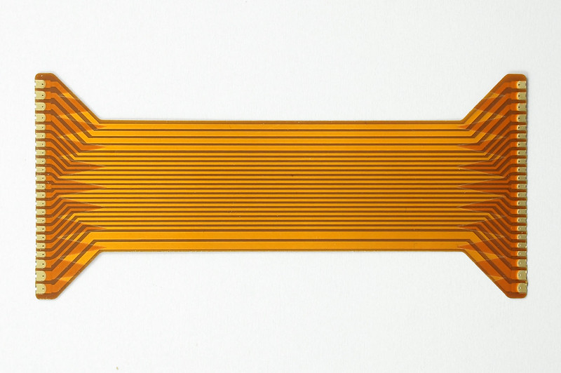
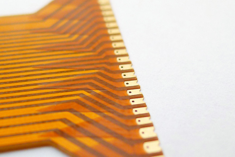
It’s a multi-layer flexible / Kapton / polyimide film PCB designed to be soldered directly to two rigid PCB’s. The key feature in the design is the addition of layers with a tapered or zig-zag design. This distributes the stress instead of creating a folding point at the edge of the rigid PCB. The additional layer makes it particularly strong at this point.

Closeup of flexible PCB connection

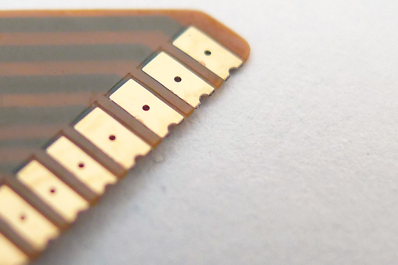
The pads are designed with a few details that make it quick and easy to solder. The top Kapton layer overlaps the pads with a radius, castellated ends are used and vias are present in the middle of the pads. These features allow the solder to easily flow under and through to the underside.

Underside of pads

The underside pad shape is extended to match the rigid PCB footprint.

Flexible PCB collection soldered on to a rigid PCB

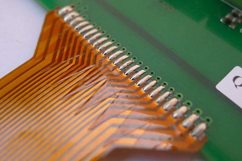
Once soldered, it gives a solid joint that is extremely durable. It can be soldered at any angle, giving more design freedom in positioning the PCB’s.  It worked out quite a bit cheaper than any other alternative in this application, even after the additional assembly process. It is particularly suitable for any application that requires high reliability.

To simplify the process I have written a piece of software that generates the connector design as an Eagle script from a range of parameters automatically.

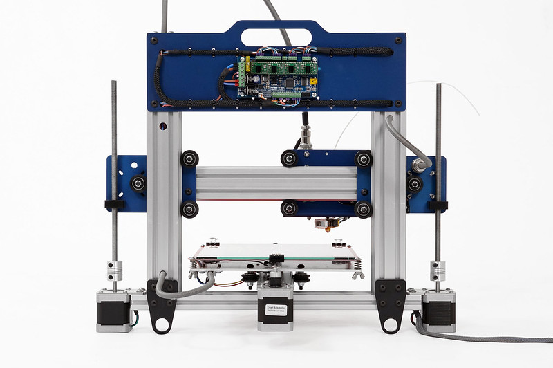
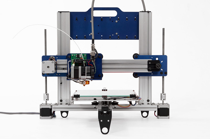
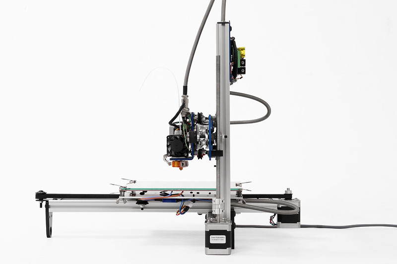
Hadron ORD Bot 3D Printer Build

This is my first 3D printer build based on the Hadron ORD bot design. It’s made from an extrusion called MakerSlide which allows the design to be pretty low cost and robust. Because of the hollow profile it allows most cable routing to be run through the centre of the profiles, keeping the build nice and clean.

Hadron ORD 3D Printer Back

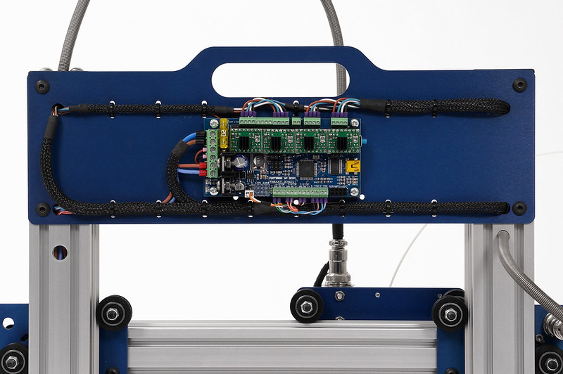
For the electronics, I chose the Azteeg X1. It’s low cost and tiny. It can run most available firmware and fully integrates everything needed. The standard connectors have been swapped for 0.1″ screw terminals.

Hadron ORD 3D Printer Front

The Stepstruder MK7 is used as the extruder. It takes 1.75mm filament and comes with a stock nozzle with an extrusion diameter of 0.4mm. The small PCB above the extruder (MakerBot safety cutoff switch) is a hardware safety cut off designed to cut power if the extruder overheats for any reason.

Hadron ORD 3D Printer Side

All of the cabling is run through 8mm stainless steel extension springs. By using proper connectors throughout, the idea is that every moving part can simply be unplugged, rather than having to be desoldered or other less than ideal solutions. A standard multipole connector was used for motors and the extruder, JST-XH used for the bed limit switch / bed thermistor and a high current EC3 connectors (rated at 60A continuous) for the heatbed 12V supply.

A few improvements were made to the standard Hadron mechanics including swapping the default 1mm steel motor mounts for 3mm stainless steel laser cut brackets and flexible motor couplers. A new modified laser cut bed mount was designed to include cable routing and spring clamps.

Azteeg X1 on Hadron ORD 3D Printer

The cabling was a mix of LÜTZE Superflex 4 core cable for motors, twisted pairs from a good quality ethernet cable and high temperature silicone cable for the heat bed. 

Inside Apple’s new folding USB Charger (UK Plug) / Teardown

The new UK USB charger (part #  MGRL2B/A) includes a folding pin design – but isn’t that much bigger than a standard charger.

apple-folding-uk-charger-cut-in-half

Rather than prying the mouldings apart and potentially damaging something in the process, I cut the rear casing in two using a fine toothed coping saw. Luckily I cut in exactly the right spot so it comes apart cleanly. It’s designed in two halves – the front half containing all of the mechanism and insulation and the second half containing the PCB with active components and USB socket.

The PCB

apple-folding-uk-charger-bottom-with-cover

The rear half of the housing has some copper shielding behind a plastic film – presumably to meet EMC standards.

apple-folding-uk-charger-pcb-top

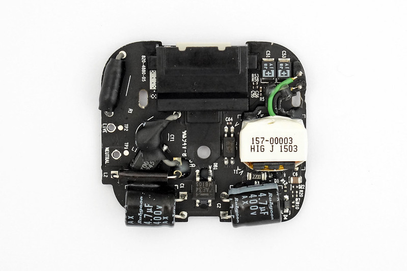
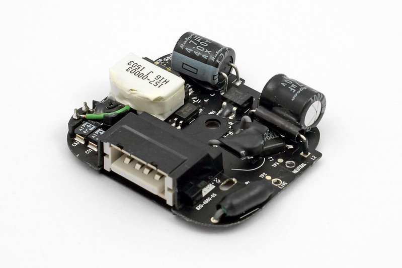
The top of the PCB and USB socket moulding is secured using a single M2.5 torx head screw. Other bits are the Rubycon AX series electrolytic capacitors, (part # 400AX4.7M8X9), Fairchild bridge rectifier (part # MB10S), Everlight optoisolator (part # EL3H7-G) and a transformer (markings 157-00003 / HIG J 1503).

apple-folding-uk-charger-top-pcb-top-perspective
apple-folding-uk-charger-pcb-bottom-perspective
apple-folding-uk-charger-pcb-bottom

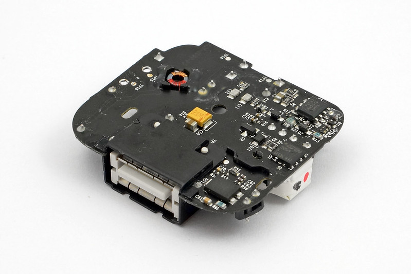
On the underside there’s a low profile, recessed inductor (markings T00405 SP451), a tantalum polymer capacitor from Kemet (part # T520T156M006ATE100 ) and what I think is a power MOSFET from Fairchild (part # STD7NM64N) but in a custom package, Fairchild’s PowerFLAT 5×5 package. The other large component is a diode (part # SBR8U60P5). Interestingly there is a blob of resin over R9 for an unknown reason.

What is surprising is the use of a low power PWM controller from Fairchild (part # FAN301). The FAN301 was released in 2010 and achieves a standby power of less than 20mW. It is currently marked as ‘This particular part was found to be patent infringing and we are unable to sell this product.‘ on Mouser. It appears to have been replaced by the FAN302 in 2013 – achieving a standby power of half; just 10mW. I’m not exactly sure why they are using this PWM controller for the above reasons, but it does hint that this charger design was a long time in the making. The FAN301 has a permanent injunction against it from Power Integrations (more on the story here).

apple-folding-uk-charger-assembly-cross-section

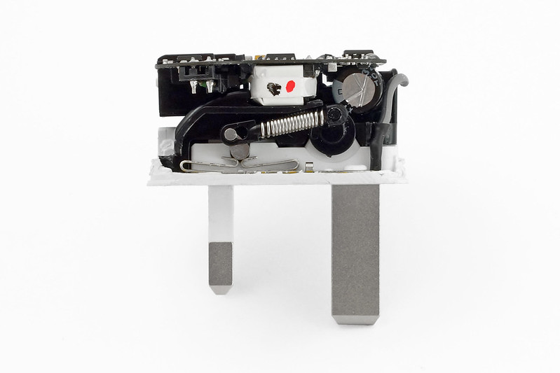
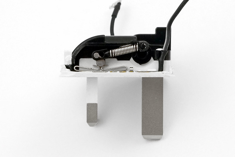
Cutting away the side of the charger face reveals the contacts.

The Mechanism

apple-folding-uk-charger-folding-mech
apple-folding-uk-charger-folding-mech-perspective-2
apple-folding-uk-charger-box-folding-mech-perspective
apple-folding-uk-charger-folding-mech-cross-section-folded-in
apple-folding-uk-charger-folding-mech-cross-section
apple-folding-uk-charger-mech-inside-top

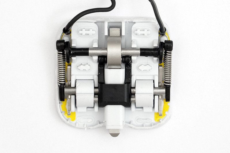
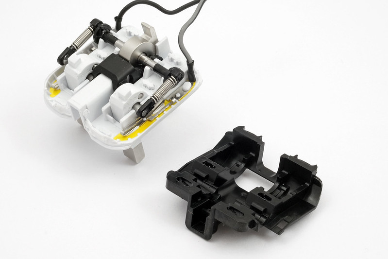
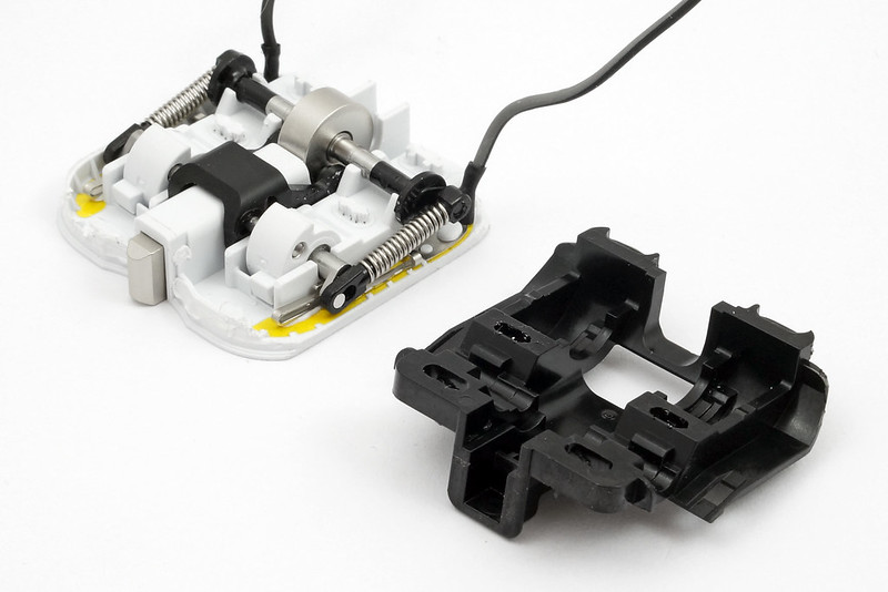
The top cover has been fixed in place using overmoulding – once these overmoulded points are cut off, you can finally see underneath the cover! All of the parts feel solid and there’s very little play when the mechanism moves.

apple-folding-uk-charger-folding-mech-inside-pins-out
apple-folding-uk-charger-folding-mech-inside

Underneath each mains contact is a thin layer of Polyimide (the yellow material) cut to shape – This is a high temperature, electrically insulating film. At a guess this is to meet insulation requirements.

Check the Apple folding plug teardown on iFixit!